Semiconductor
ENERGY BANDS IN SOLIDS
The range of energy possessed by electron in a solid is called energy band.
1. Valence Band
The band formed by a series of energy levels
containing the valence electrons is known as valence band. The valence band may
be defined as a band which is occupied by the valence electrons or a band
having highest occupied band energy. It may be completely or partially filled
but never be empty.
2. Conduction Band
The range of energy possessed by electrons that are
responsible for conduction is called conduction band. It may be empty or
partially filled.
3. Forbidden Band
The separation between conduction
band and valence band is known as forbidden energy gap. There is no allowed
energy state in this gap and hence no electron can stay in the forbidden energy
gap.
Insulators, Semiconductors and Conductors
Insulators
Semiconductors
Conductors

SEMICONDUCTORS
A substance which has conductivity in between conductors and insulators is known as semiconductor. Semiconductors have the following properties.
(i) They have resistivity less than insulators and more than conductors.
(ii) The resistance of semiconductor decreases with the increase in temperature and vice versa.
(iii) When suitable metallic impurity like arsenic, gallium etc. is added to a semiconductor, its current conducting properties change appreciably.
Effect of temperature of Semiconductors
At very low temperature (say 0 K) the semiconductor crystal behaves as a perfect insulator since the covalent bonds are very strong and no free electrons are available. At room temperature some of the covalent bonds are broken due to the thermal energy supplied to the crystal. Due to the breaking of the bonds, some electrons become free which were engaged in the formation of these bonds.The absence of the electron in the covalent bond is represented by a small circle. This empty place or vacancy left behind in the crystal structure is called a hole. Since an electron has a unit negative charge, the hole carries a unit positive charge.
Mechanism of conduction of Electrons and Holes

There is a strong tendency of semiconductor crystal
to form covalent bonds. Therefore, a hole attracts an electron from the
neighboring atom. Now a valence electron from nearby covalent bond comes to
fill in the hole at A. This results in a creation of hole at B. The hole has
thus effectively shifted from A to B. This hole move from B to C from C to D
and so on.
This movement of the hole in the absence of an
applied field is random. But when an electric field is applied, the hole drifts
along the applied field.
Depending on the type of impurities added,
semiconductor is divided into two types:
1) Intrinsic Semiconductor and
2) Extrinsic Semiconductor
Intrinsic Semiconductor
A semiconductor in an extremely pure from is known
as intrinsic semiconductor or a semiconductor in which electrons and holes are
solely created by thermal excitation is called a pure or intrinsic
semiconductor. In intrinsic semiconductor the number of free electrons is
always equal to the number of holes.
Extrinsic Semiconductor
The electrical conductivity of intrinsic
semiconductor can be increased by adding some impurity in the process of
crystallization. The added impurity is very small of the order of one atom per
million atoms of the pure semiconductor. Such semiconductor is called impurity
or extrinsic semiconductor. The process of adding impurity to a semiconductor
is known as doping.
The doping material is either pentavalent atoms
(bismuth, antimony, arsenic, phosphorus which have five valence electrons) or
trivalent atoms (gallium, indium, aluminium, boron which have three valence
electrons). The pentavalent doping atom is known as donor atom because it donates
one electron to the conduction band of pure semiconductor.
The doping materials are called impurities because
they alter the structure of pure semiconductor crystals.
Depending on the types of impurities added, the
extrinsic semiconductor is divided into two types: 1) N- type Semiconductor and
2) P- type semiconductor
N–Type Semiconductor
When a small amount of pentavalent impurity is added
to a pure semiconductor crystal during the crystal growth, the resulting
crystal is called as N-type extrinsic semiconductor.

In case of N-type semiconductor, the following
points should be remembered
(i)
In N-type semiconductor, the electrons are the
majority carriers while positive holes are minority carriers.
(ii)
Although N-type semiconductor has excess of
electrons but it is electrically neutral. This is due to the fact that
electrons are created by the addition of neutral pentavalent impurity atoms to
the semiconductor i.e., there is no addition of either negative changes or
positive charges.
P–Type Semiconductor
When a small amount of trivalent impurity is added
to a pure crystal during the crystal growth, the resulting crystal is called a
P-type extrinsic semiconductor.
In case of P-type semiconductor, the following
points should be remembered
(i)
In P-type semiconductor materials, the majority
carriers are positive holes while minority carriers are the electrons.
(ii)
The P-type semiconductor remains electrically
neutral as the number of mobile holes under all conditions remains equal to the
number of acceptors.

P-N Junction Diode
When a P-type material is intimately joined to
N-type, a P-N junction is formed. In fact, merely-joining the two pieces a P-N
junction cannot be formed because the surface films and other irregularities
produce major discontinuity in the crystal structure. Therefore a P-N junction
is formed from a piece of semiconductor (say germanium) by diffusing P-type
material to one half side and N-type material to other half side. When P-type
crystal is placed in contact with N-type crystal so as to form one piece, the
assembly so obtained is called P-N junction diode.

Biasing of a diode
Forward Biased PN Junction Diode

When a diode is connected in a Forward Bias condition, a negative voltage is applied to the N-type
material and a positive voltage is applied to the P-type material. If this
external voltage becomes greater than the value of the potential barrier,
approx. 0.7 volts for silicon and 0.3 volts for germanium, the potential
barriers opposition will be overcome and current will start to flow.
Reverse Biased PN Junction Diode

When a diode is connected in a Reverse Bias condition, a positive
voltage is applied to the N-type material and a negative voltage is applied to
the P-type material.
The positive voltage applied to the N-type material
attracts electrons towards the positive electrode and away from the junction,
while the holes in the P-type end are also attracted away from the junction
towards the negative electrode. The net
result is that the depletion layer grows wider due to a lack of electrons and
holes and presents a high impedance path, almost an insulator and a high
potential barrier is created across the junction thus preventing current from
flowing through the semiconductor material.
Characteristics of a diode
Forward Characteristic for a Junction Diode 
Reverse Characteristic for a Junction Diode

Rectification
The process of converting an ac signal into dc signal is called rectification. An electronic device which converts a.c. power into d.c. power is called a rectifier.
Half wave rectifier
Principle
Junction diode offers low resistive path when forward
biased and high resistance when reverse biased.

Arrangement
The a.c. supply is fed across the primary coil (P)
of step down transformer. The secondary coil ‘S' of transformer is connected to
the junction diode and load resistance RL. The output d.c. voltage
is obtained across RL.
Theory
During first half of a.c. input cycle the junction
diode gets forward biased. The conventional current will flow in the direction
of arrowhead. The upper
end of
RL will be at +ve potential w.r.t. the
lower end. The magnitude of output across RL during first half at
any instant will be proportional to magnitude of current through RL,
which in turn is proportional to magnitude of forward bias and which ultimately
depends upon the value of a.c. input at that time.

Full wave rectifier
A rectifier which rectifies both halves of a.c.
input is called full wave rectifier.
Principle
Junction Diode offers low resistive path when
forward biased and high resistive path when reverse biased.
Arrangement
The a.c. supply is fed across the primary coil (P)
of step-down transformer. The two ends of S–coil (secondary) of transformer is
connected to P-section of junction diodes D1 and D2. A
load resistance RL is connected across the n–sections of two diodes and central
tapping of secondary coil. The d.c. output is obtained across RL.
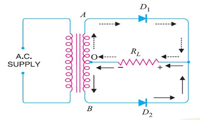
Theory
During first half of input cycle upper end of s-coil
is at +ve potential. The junction diode D1 gets forward biased,
while D2 gets reverse biased. The conventional current due to D1
will flow along path of full arrows. When second half of input cycle comes, the
conditions will be exactly reversed. Now the junction diode D2 will
conduct and the conventional current will flow along path of dotted arrows.
Since current during both the half cycles flows from
right to left through load resistance RL, the output during both the
half cycles will be of same nature.
The right end of RL is at +ve potential
w.r.t. left end. Thus in full wave rectifier, the output is continuous.

Zener Diode
A Zener diode is a heavily doped semiconductor
device that is designed to operate in the reverse biasing. When the voltage across the
terminals of a Zener diode is reversed and the potential reaches the Zener
Voltage, the junction breaks down and the current flows in the reverse
direction. This effect is known as the Zener Effect.
There are two types of breakdowns for a Zener
Diode:
a) Avalanche
Breakdown
b) Zener
Breakdown
Avalanche Breakdown in Zener Diode
Avalanche breakdown occurs both in normal diode and
Zener Diode at high reverse voltage. When a high value of reverse voltage is
applied to the PN junction, the free electrons gain sufficient energy and
accelerate at high velocities. These free electrons moving at high velocity
collides other atoms and knocks off more electrons. Due to this continuous
collision, a large number of free electrons are generated as a result of
electric current in the diode rapidly increases. This sudden increase in
electric current may permanently destroy the normal diode, however, a Zener
diode is designed to operate under avalanche breakdown and can sustain the
sudden spike of current.
Zener Breakdown in Zener Diode
When the applied reverse bias voltage reaches closer
to the Zener voltage, the electric field in the depletion region gets strong
enough to pull electrons from their valence band. The valence electrons that
gain sufficient energy from the strong electric field of the depletion region
break free from the parent atom. At the Zener breakdown region, a small
increase in the voltage results in the rapid increase of the electric current.

Symbol

Characteristics of Zener diode
Zener diode as a voltage regulator
To maintain a constant voltage across the load, even
if the input voltage or load current varies, voltage regulation is to be made.
A Zener diode working in the breakdown region can act as a voltage regulator.

The circuit in which a Zener diode is used for
maintaining a constant voltage across the load RL is shown in Fig.
The Zener diode in reverse biased condition is connected in parallel with the
load RL. Let Vdc be the unregulated dc voltage and VZ be
Zener voltage (regulated output voltage). RS is the current limiting
resistor. It is chosen in such a way that the diode operates in the breakdown
region.
In spite of changes in the load current or in the
input voltage, the Zener diode maintains a constant voltage across the load.
The action of the circuit can be explained as given below:
Load current
varies, the input voltage is constant: Let us consider that the load
current increases. Zener current hence decreases, and the current through the
resistance RS is a constant.
The output voltage is VZ = Vdc
– IRs, since the total current I remains constant, the output
voltage remains constant.
Input voltage
varies: Let us consider that the input voltage Vdc increases.
Now the current through Zener increases and the voltage drop across Rs
increases in such a way that the load voltage remains the same. Thus the Zener
diode acts as a voltage regulator.
Transistor
It is three sections semiconductor, in which three
sections are combined so that the two at extreme ends have the same type of
majority carriers, while the section that separates them has the majority
carriers in opposite nature. The three sections of transistor are called
emitter (E), Base (B), collector (C).
Ø Emitter-
It is heavily doped region. It emits charge carriers.
Ø Collector-
It is moderately doped region. It is largest section. It collects charge
carriers.
Ø Base-
It is lightly doped region. It passes charge carriers from emitter to
collector. It is smallest section.
Symbol
Biasing of a transistor
Ø Emitter-
Base junction is forward biased.
Ø Collector-Base
junction is reversed biased.
Action of N-P-N Transistor

Fig. shows that, the N-type emitter is forward
biased by connecting it to -ve pole of VBE (base-emitter battery)
and N-type collector is reverse biased by connected it to +ve pole of VCB
(collector- base
battery).
The majority carriers (e-) in emitter are
repelled towards base due to forward bias. The base contains holes as majority
carriers but their number density is small as it is doper very lightly (5%) as
compared to emitter and collector. Due to the probability of e- and
hole combination in base is small. Most of e- (95%) cross into
collector region where they are swept away by +ve terminal of battery VCB.
Corresponding to each electron that is swept by
collector, an electron enters the emitter from -ve pole of collector - base
battery.
If Ie, Ib, Ic be
emitter, base and collector current respectively then using Kirchoff first law,
Ie = Ib + Ic
Action of P-N-P Transistor

The p–type emitter is forward biased by connecting
it to +ve pole of emitter – base battery and p-type collector is reverse biased
by connected it to -ve pole of collection - base battery. In this case,
majority carrier in emitter i.e. holes are repelled towards base due to forward
bias. As base is lightly doped, it has low number density of e-.
When hole enters base region, then only 5% of e- and hole
combination take place. Most of the holes reach the collector and are swept
away by -ve pole of VCB battery.
Configuration of transistor
There are three types of configurations of a
transistor.
Ø Common
Emitter configuration
Ø Common
Collector configuration
Ø Common
Base configuration
Each has different properties in terms of the
gain, and input and output impedance etc and as a result, a particular
configuration will be selected during the electronic circuit design process.

Common Emitter Characteristics
The circuit diagram for common emitter
characteristics is shown in figure below.

The three important characteristics of a transistor
in any mode are (i) input characteristics (ii) output characteristics and (iii)
transfer characteristics.
(i) Input characteristics
Input characteristic curve is drawn between the base
current (IB) and voltage between base and emitter (VBE),
when the voltage between collector and emitter (VCE) is kept
constant at a particular value. VBE is increased in suitable equal
steps and corresponding base current is noted. The procedure is repeated for
different values of VCE.
IB values are plotted against VBE
for constant VCE. The input characteristic thus obtained is shown in
Fig. The input impedance of the transistor is defined as the ratio of small
change in base - emitter voltage to the corresponding change in base current at
a given VCE. Input
impedance r1 = (∆VBE/∆IB)at VCE = constant

(ii) Output characteristics
Output characteristic curves are drawn between IC
and VCE, when IB is kept constant at a particular
value.
The base current IB is kept at a constant
value, by adjusting the base emitter voltage VBE. VCE is
increased in suitable equal steps and the corresponding collector current is
noted. The procedure is repeated for different values of IB. Now, Ic
versus VCE curves are drawn for different values of IB.
Output impedence, ro = (∆VCE/ ∆IC)at IB=constant

(iii) Transfer characteristics
The transfer characteric curve is drawn between IC
and IB, when VCE is kept constant at a particular value.
The base current IB is increased in suitable steps and the collector
current IC is noted down for each value of IB. The
transfer characteristic curve is shown in Fig.

The current gain is defined as the ratio of a small
change in the collector current to the corresponding change in the base current
at a constant VCE.
Current
gain, β = (∆IC/ ∆IB)VCE
The common emitter configuration has high input
impedance, low output impedance and higher current gain when compared with
common base configuration.
Alpha(α) and (β) parameter of a transistor.

This is relation between α and β.
CE Amplifier

Circuit diagram for CE amplifier is shown in figure
above. From figure,
IE = IB + IC
and
VCE = VCC – ICRC
When the positive half cycle of input a.c. signal
voltage comes, it supports the forward biasing of the emitter-base circuit. Due
to this, the emitter current increases and consequently the collector current
increases. As a result of which, the collector voltage Vc decreases.
Since the collector is connected to the positive
terminal of VCE battery, therefore decreases in collector voltage
means the collector will become less positive which means negative w.r. to
initial value. This indicates that during positive half cycle of input a.c.
signal voltage, the output signal voltage at the collector varies through a
negative half cycle.
When negative half cycle of input a.c. signal voltage comes, it opposes the forward biasing of emitter-base circuit, due to this the emitter current decreases and hence collector current decreases; consequently, the collector voltage Vc increases i.e., the collector becomes more positive. This indicate that during the negative half cycle of input a.c. signal voltage, the output signal voltage varies through positive half cycle.
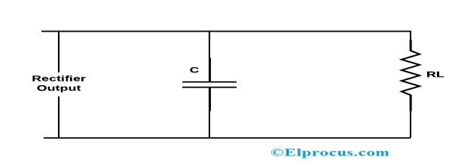
Filter Circuit
The filter is a device that allows passing the dc
component to the load and blocks the ac component of the rectifier output. Thus
the output of the filter circuit will be a steady dc voltage. The filter
circuit can be constructed by the combination of components like capacitors,
resistors, and inductors. Some of commonly used filter circuits are:
i)Induction filter ii) Capacitor filter iii) LC filter iv) ![]() – filter etc.
– filter etc.
Inductor filter